Laser Chip Cutting Technology

Related types: Solutions
Release time:2026-03-09
Return to List

Laser Chip Cutting Technology

Against the backdrop of continuous miniaturization and integration across the optoelectronics industry, optoelectronic chips and components feature increasingly intricate microstructures and geometries, along with ever-stringent machining precision requirements. Conventional processing techniques are inadequate for machining millimeter and even micrometer-level special-shaped structures, suffering from insufficient precision, low efficiency, and unstable yield rates.
These flaws have become core bottlenecks restricting product innovation and mass production in the optoelectronics field. Achieving high-precision and high-efficiency chip cutting has thus become an urgent key problem for optoelectronic enterprises to solve.

Ⅰ. Addressing Industry Pain Points: Dual Challenges of Micro Precision and Complex Special-Shaped Machining

Optoelectronic chips and core components such as optical filters, sensor wafers, micro lens arrays, and optical waveguide devices are characterized by special material properties, refined structures, and complex shapes. Traditional mechanical processing and ordinary laser cutting technologies commonly face the following pain points in actual production:

1.Precision Defects Leading to Component Performance Failure

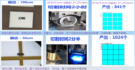
Tiny edge chipping, microcracks, and expanded heat-affected zones (HAZ) generated during cutting will directly change the physical and optical properties of optoelectronic chips, resulting in functional failure and scrapped products.

2.Difficult Machining of Complex Special-Shaped Structures

For non-standard curved contours, micro inner corners, and ultra-narrow slits of chip structures, traditional processes require cumbersome programming procedures and deliver poor machining consistency, making it impossible to support stable and standardized mass production.

3.Low Efficiency and High Production Cost Pressure
Traditional processing features high trial-and-error costs and long single-piece processing cycles, failing to adapt to the rapid iteration and large-scale delivery demands of optoelectronic products, and greatly limiting the core competitiveness of enterprises.

Ⅱ.Hirundo Laser Chip Cutting Solution: Three-Dimensional Empowerment for High-Precision Machining

Targeting the above industry pain points, Hirundo launches an integrated laser chip cutting solution integrating high-precision hardware equipment, intelligent algorithm systems, and full-process production optimization, providing enterprises with full-link technical support from prototype verification to large-scale batch production.

1.High-Precision Laser Cutting Equipment: Solid Hardware Foundation for Chip Machining
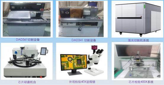
We adopt self-developed high-power ultrashort pulse (picosecond/femtosecond) lasers, matched with high-rigidity granite platforms, high-response linear motor drive systems, and nanoscale grating closed-loop feedback systems, to build an ultra-stable professional chip machining platform.

Superior Cold Machining Performance

The ultrashort pulse laser realizes nearly zero-heat cold cutting, which greatly suppresses the generation of heat-affected zones. It is highly adaptable to thermosensitive and brittle chip materials such as sapphire, special optical glass, ceramic substrates, and compound semiconductors, effectively avoiding material melting, microcracks, and structural denaturation, and ensuring the integrity of chip optical and electrical properties.

Ultra-High Precision Motion Control

The linear motor drive system ensures stable operation under high speed and high acceleration. The nanoscale closed-loop positioning system keeps the long-term positioning accuracy of the workbench within ±1μm, providing accurate physical support for micron-level chip cutting.
2.Intelligent Cutting Algorithm System: Core Software Driving Force for Complex Machining
Hardware determines the machining foundation, while intelligent algorithms define the cutting quality. Our self-developed software system is the core advantage of the chip cutting solution:

Intelligent Contour Path Planning

Aiming at the complex special-shaped contours of optoelectronic chips, the system algorithm automatically optimizes cutting paths, prioritizes difficult processing areas such as tiny inner corners and sharp vertices, and ensures complete and consistent chip contour dimensions. For batch repetitive chip graphics, it supports intelligent typesetting and path merging, eliminating idle strokes and greatly improving processing efficiency.

Adaptive Material Parameter Database

The system is embedded with a massive process parameter database covering mainstream chip materials. Combined with real-time visual monitoring feedback, it can adaptively fine-tune laser power, repetition frequency, scanning speed and other core parameters. For new special chip materials, it can quickly match the optimal processing scheme through a small number of tests, shortening the process debugging cycle.

Dynamic Focusing and Beam Shaping Technology

Equipped with a high-performance dynamic focusing system, it maintains consistent laser focus characteristics in the full processing range. The optional beam shaping module can optimize the laser spot distribution according to chip material and structural characteristics, further improving cutting flatness and dimensional accuracy.

3.Batch Production Process Optimization: Realize Efficient and Stable Mass Manufacturing

We optimize the laser chip cutting process from the overall production link, realizing the upgrade from single-point high precision to full-line high efficiency:

Automatic Loading and Unloading Integration

The equipment can be seamlessly connected with robotic arms, AGVs and other automatic equipment to realize automatic positioning, cutting and unloading of chip wafers and substrates. It minimizes manual intervention, eliminates human error, and ensures 24-hour stable continuous production.

Online Real-Time Monitoring and Quality Traceability

Integrated high-resolution CCD visual inspection system, realizing pre-processing automatic deviation correction, in-process real-time quality monitoring, and post-processing precision size detection. All processing data is automatically recorded and traceable, providing reliable data support for process optimization and quality control.

MES System Docking

Equipment operation status and chip processing data can be directly uploaded to the customer's MES production management system, realizing transparent production progress, real-time equipment efficiency analysis and predictive maintenance reminders, and improving the overall intelligent production level.

4.Core Advantages of Hirundo Chip Cutting Technology: Professional Strength Defined by Data

Ultimate Machining Precision

The comprehensive cutting accuracy is controlled within ±5μm, with smooth and burr-free chip kerfs, excellent sidewall verticality and ultra-small heat-affected zones. It effectively improves the consistency and operational reliability of optoelectronic chip performance.

Significant Efficiency Improvement

Compared with traditional processing technology, the batch processing efficiency of chips is increased by more than 30%. Intelligent typesetting and high-speed motion control shorten single-piece processing time, and automatic production lines greatly reduce auxiliary working hours.

Wide Material Adaptability

It is applicable to various chip materials such as metal substrates, ceramics, optical glass, crystal materials, polymers and composite materials, and is especially suitable for high-hardness, high-brittleness and multi-layer composite optoelectronic chip precision processing scenarios.

Lower Comprehensive Production Cost

Ultra-high yield reduces material waste, efficient processing cuts unit time cost, and automated production reduces labor dependence. It comprehensively reduces the overall production and operation costs of enterprises.

.Conclusion

In the rapid iteration and upgrading of optoelectronic technology, ultra-precision chip machining capability is the core foundation for technological innovation and product iteration. Hirundo laser chip cutting technology is not only a set of processing equipment, but also a systematic intelligent manufacturing platform integrating precision engineering, intelligent algorithms and lean production management.

We help enterprises break through the bottlenecks of complex-shaped and micro-sized chip processing, implant precision, efficiency and stability into every production link, and jointly promote the optoelectronic chip industry to develop towards miniaturization, integration and high precision.

Choose Hirundo, Cut Boundless Possibilities.